非制冷熱傳感器技術與進出口
很多人和很多客戶不是很清楚為什么有些熱像儀進口非得要中國商務部和熱像儀生產國商務部的批準證書,經常對此提出疑問,請大家仔細看看本網頁的說明。
實際上,熱像儀如果是非制冷微型熱輻射計探測器和幀頻大于9Hz,那么就必須要獲得中國商務部和生產國商務部的批準,才可以出口。
A paradigm shift has occurred in the commercial infrared camera industry as a result of classified military thermal sensor development in the 1980’s. In the past most high performance infrared cameras used in commerce had photon-detection sensors that needed to be cooled to liquid nitrogen temperature (77K). Cryogenic coolers were used to cool the detectors requiring about 10 minutes turn-on time to achieve this very low temperature. New high performance cameras use thermal sensors that eliminate the need for cryo-coolers. Their turn-on time is 15 seconds or less.
Cryo-coolers are expensive and have wear-out issues. The elimination of the cryo-cooler and advances in electronics has made the cameras smaller, more reliable and less expensive.
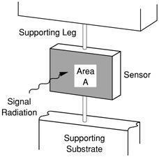
熱傳感器
紅外熱傳感器原理圖如右圖所示。A tiny thin plate (which I call a “platelet”) is made on a silicon wafer in a silicon foundry by a micro-machining process. The platelet is typically 50 m (microns) square by 0.5 m thick. Even smaller sizes are under development. Long thin support legs and a vacuum environment thermally isolates it from the substrate. Small thermal radiation from the target focused onto the platelet heats it. The higher the target temperature, the greater the focused radiation is and therefore the higher the platelet temperature.
The temperature of the platelet and therefore the intensity of the radiation can be measured by the change in resistance of an electrical resistor deposited on the platelet -- the microbolometer sensor. It can be measured by a thermocouple with the hot junction on the platelet and the reference junction on the substrate -- the thermoelectric sensor. Or it can be measured by an electrical capacitance effect -- the pyroelectric sensor. The microbolometer was developed by Honeywell and is used in Infrared Solutions, Inc. cameras.
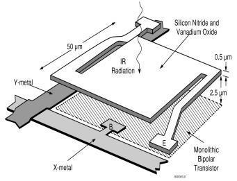
微型測輻射熱儀技術
| Individual sensor elements use the change in electrical resistance of a VOx resistor deposited onto the tiny “platelets” fabricated by silicon micro-machining in a silicon foundry. Incoming target radiation heats the VOx causing a change in electrical resistance, which is readout by measuring the resulting change in bias current. 80,000 and more sensors can be fabricated together into a two-dimensional array. The structure can be dimensioned to operate at 30 Hertz. That is, the thermal conductance of the isolating legs can be adjusted to match the time-constant for 30-hertz operation. An example of a microbolometer element is pictured below. | |
| It consists of a two-layer structure. An interconnecting readout circuitry is applied to the silicon process wafer and then the microbolometer structure is built on top of the readout circuitry. First a pattern of islands _ wavelength thick are deposited on the readout circuitry. The islands are made of a material that can be selectively etched away later to form a bridge structure. Three layers -- silicon nitride, vanadium oxide, and silicon nitride -- are deposited over the sacrificial islands. The sacrificial islands are then etched away leaving the thermally isolated bridge structure of vanadium oxide. A photo of an early Honeywell microbolometer element is shown in the picture below followed by a photo of one corner of a 320 by 240 microbolometer array |
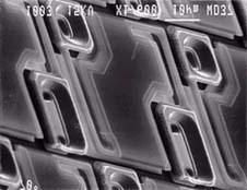
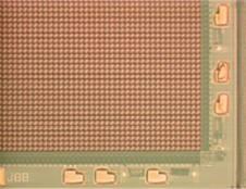
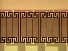
現在大多數熱像儀制造商都使用320x240像素的微型熱輻射儀陣列探測器。然而依然有一款極優越的可替代品-160x120的陣列探測器,雖然陣列小,但制造出的熱像儀價格卻價格低很多。更多Far more arrays can be produced on a single wafer and the yield is higher for the smaller array. In addition, one of the most expensive components of an infrared camera is the lens and its cost is proportional to the array size.
The only advantage of the larger array is field of view (FOV). With the same f# and focal length lens and the same detector size, a camera with 320 by 240 or 160 by 120 will have identical spatial resolution. But the target size for a fixed distance between the camera and target will be twice as large in both dimensions for the camera with the larger array. For many commercial applications the cost savings of the smaller array size over shadows the advantage of a larger FOV.
20世紀80年代,美國國防部給Honeywell和Texas Instruments (TI) 2個公司很多大型機密的合同,開發非制冷紅外傳感器技術。軍事用途要求一種傳感器可以極短時間能工作。這2個計劃都非常成功,TI公司開發出了焦熱電傳感器,Honeywell公司開發出了微型測輻射熱儀(微型熱輻射儀)。
1992年美國政府為商用產品從機密表中刪除了紅外技術的應用一項,但保留了對技術的控制。TI公司利用它們的傳感器技術開發出了商用熱像儀,Honeywell則開始向其它公司發放許可證允許他們使用微型測熱輻射儀技術。
最初有4個公司購買了微型測熱輻射儀使用證書。Loral公司收購了Honeywell的 光電部門(Electro Optics Division),獲得了一個使用證書。Santa Barbara Research是Hughes, Amber Engineering的一個部門, 與Amber Engineering及Rockwell也都購買了使用證書。所有這4個證書也都曾經轉手過,而且有些還不止一次。Loral后來被Lockheed Martin收購, Lockheed Martin后來將微型測熱輻射儀機構應用到他們的Sanders運作中,而這個項目后來又被英國航天航空(British Aerospace)收購。Raytheon (雷神)則從Hughes收購了Santa Barbara Research并收購了Amber Engineering。波音公司收購了Rockwell的紅外機構,幾年以后又把它賣給了DRS技術公司。所以最初的4個有證書的公司目前變成了3個:英國航天航空(British Aerospace), Raytheon(雷神)和DRS技術公司(DRS Technologies)。
有3個另外的公司也購買了使用證書,分別是Indigo Systems, InfraredVision技術公司以及最新購買的公司NEC。除了這6個公司,Institut National d’Optique (INO), 有有限使用的證書。
過去紅外熱像儀多使用特殊材料制成的傳感器,這些特殊材料需要帶液態氮冷卻,冷卻溫度可到-320℉ (-195℃)。這方面的技術突破是因為軍事研發取得的,使得生產非制冷、高性能的測量和傳感紅外能量的傳感器成為可能。這種新型非制冷技術受商業用途的刺激,使得紅外技術的應用顯現出巨大的商機。
這種非制冷技術也使得開發新型、低成本、易操作的2維探測器紅外成像設備成為可能。這種紅外成像設備,如德國DIAS紅外系統公司的便攜式熱像儀MIDAS 320L或PYROVIEW 320/380/640N等設備,可以立即“看到”整個景色,可以在視頻設備中產生實時的圖像。
下一篇:雙色紅外探測器的現狀與發展
